
Engineered air cavities dramatically enhance emission in atom-thin semiconductors
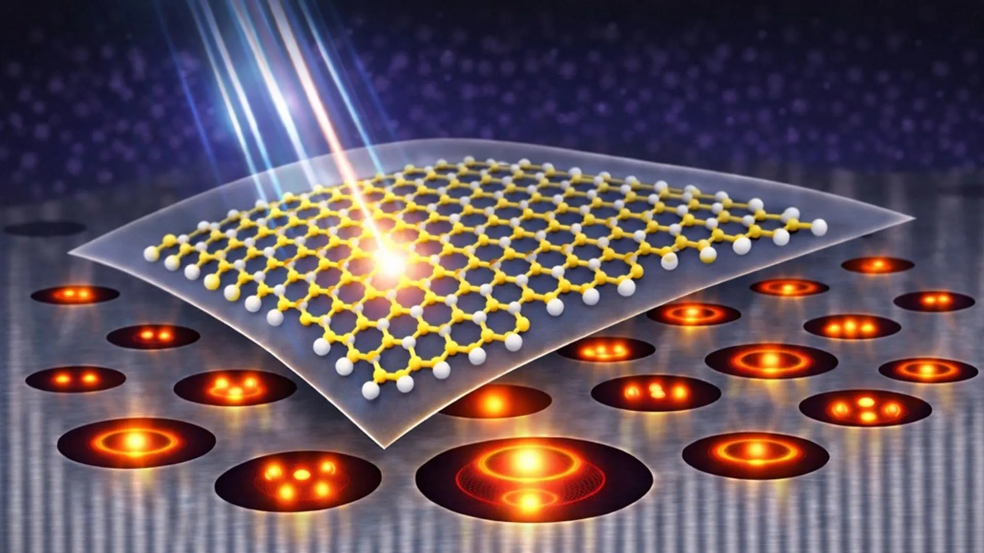
 Researchers have developed a novel approach to significantly boost the optical performance of atomically thin semiconductors without altering the material itself. By placing a single-layer tungsten disulfide (WS2) over nanoscale air cavities, called Mie voids, etched into bismuth telluride (Bi2Te3), they created highly efficient light traps. Unlike traditional dielectric resonators that confine light within solid materials, Mie voids trap light in subwavelength air cavities, concentrating the optical field exactly where the WS2 layer sits. This ‘inverted’ confinement leads to up to 20 times stronger photoluminescence and 25 times enhanced nonlinear optical signals. The cavities were precisely designed through electromagnetic simulations and fabricated using focused ion beam milling, allowing for tunable resonances that align with WS2 exciton emission. Measurements confirmed that the enhanced emission is due to the engineered cavity modes rather than material variations, and the setup also enables visualization of localized optical modes in real space. This technique opens new avenues for applications in quantum optics, on-chip light sources, nonlinear photonics, and surface-enhanced sensing, demonstrating that careful engineering of empty space can rival traditional material modifications in controlling light-matter interactions at the nanoscale.