
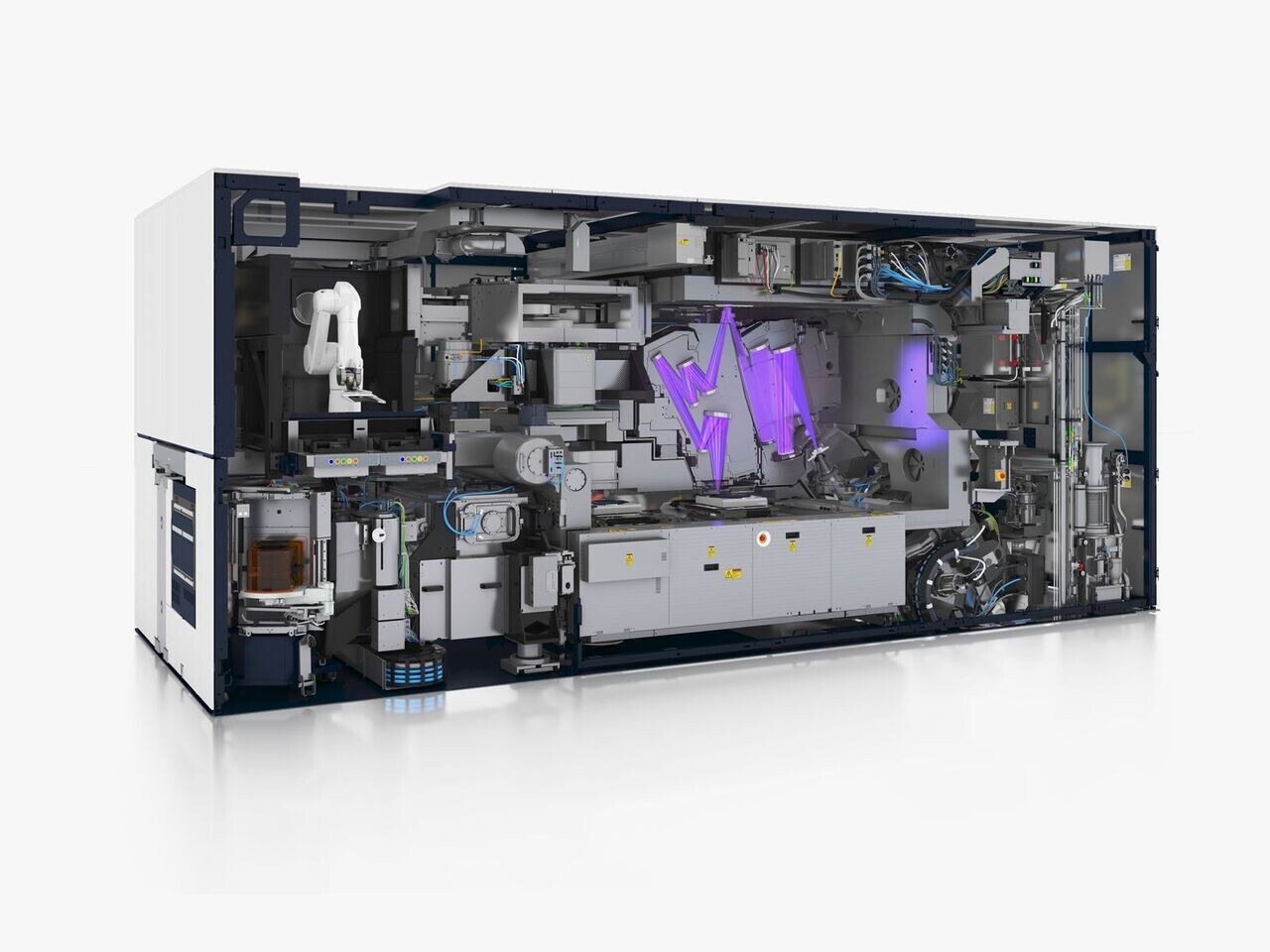
China Tests Domestic EUV Lithography Prototype Developed with Reverse-Engineered Components
According to sources close to Reuters, China has developed a functional prototype of an EUV lithography machine, currently undergoing testing. This achievement is attributed to Chinese companies, including Huawei, who successfully reverse-engineered ASML’s advanced EUV scanners and built a domestic version using second-hand parts. The prototype reportedly occupies a full factory floor, similar in size to modern High-NA EUV machines from ASML. The Chinese government initially targeted 2028 for producing working chips with this machine, but progress suggests it may come sooner. Huawei is leading this initiative to establish a complete domestic AI and semiconductor supply chain, reducing dependence on foreign technologies. The prototype employs laser-induced discharge plasma (LDP) technology to generate 13.5 nm EUV light, offering potential advantages over ASML’s laser-produced plasma (LPP) systems, such as reduced footprint, improved energy efficiency, and lower costs. The machine is now reportedly producing initial wafers for lab testing. Chinese companies involved must now ensure the system meets performance standards, including resolution, throughput stability, and integration with existing fabrication processes. The success of this project could significantly impact the global semiconductor industry and challenge ASML’s long-standing dominance in EUV lithography.